Z80 diagrams (2)
 back to page 1
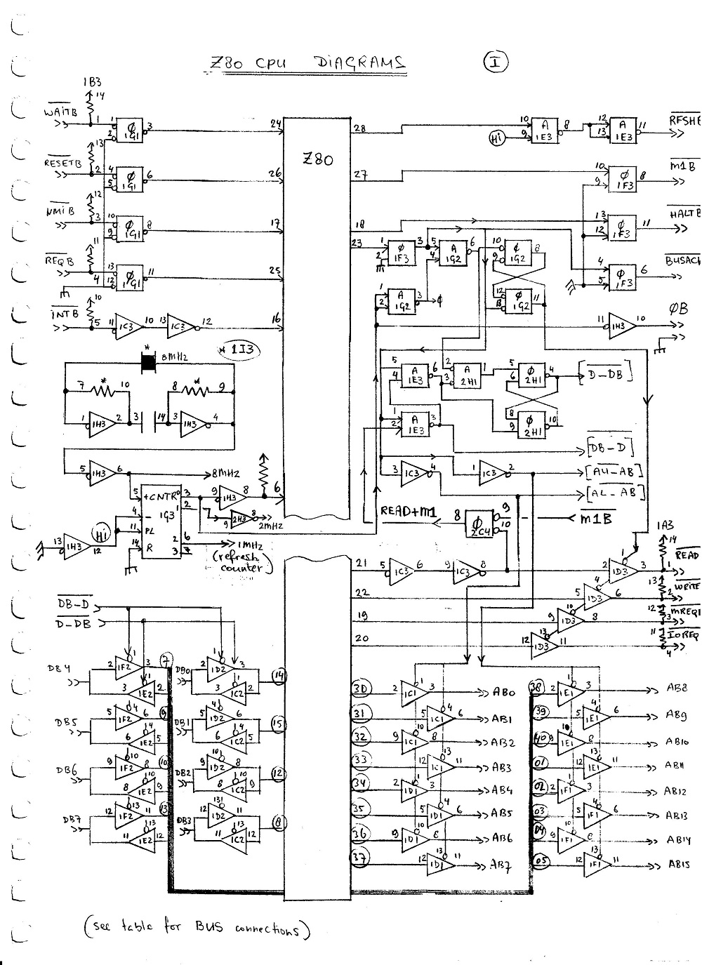
Signals xxxB are part of the bus.
Data and address are tri-state.
Pull up resisters on the bus secure HI (control off) levels.
Memory
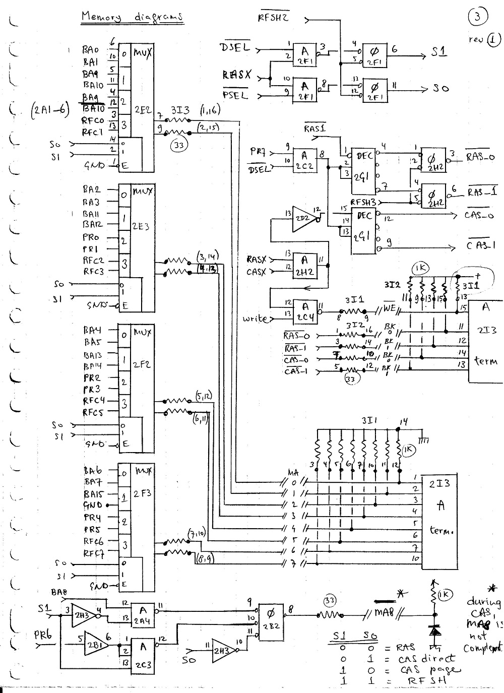
Memory consists of 16 256K*1 dynamic memory chips : 512 kilobytes.
The Z80 processor can access 64KB.
In my Z80 project, I allow the Z80 to address the first 48K (0000..BFFF hexadecimal) directly.
Addresses D000..FFFF are occupied by three EPROMs, containing the operating system.
I/O addressing is not used.
Instead, addresses C000..CFFF give access to various registers such as the console data,
address and breakpoint registers, I/O ports and also an 8 bit page register at address CExx.
The memory is divided into 256 pages of 2K bytes.
Addresses C400..CBFF form a 2k byte window to read the page selected.
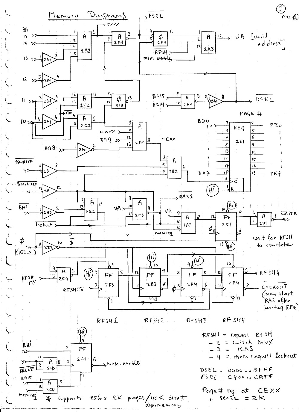
The memory control must take care of refreshing the dynamic ram chips and also requests from the console.
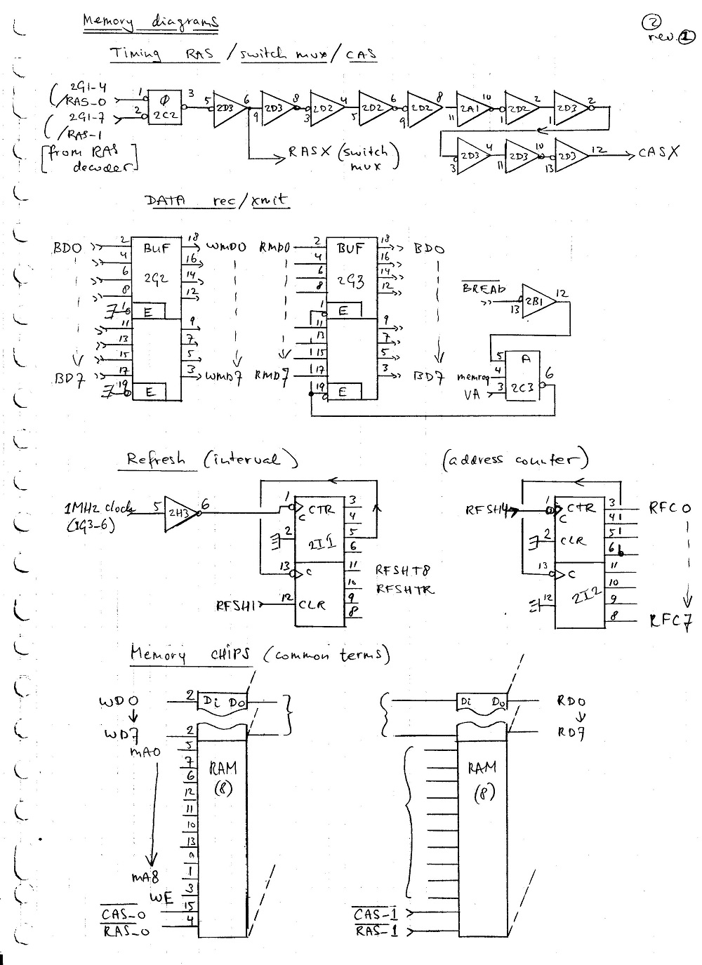
Shows refresh circuitry.
END (so far)