Z80 Diagrams
Early '80s I build a home computer around the newly available Z80 single chip processor.
The idea was to start from scratch:
Code had to be entered into memory by hand.
For debugging purposes instructions should be executed step-by-step,
breakpoints should be set on instruction read and operand read or write.
For this purpose a console with LED displays and switches was attached to the bus.
This console could "steal" cycles from the processor to access memory during program execution.
The project involved some 400 TTL (low power Schottky) chips wich I bought second hand.
The chips were placed in wire-wrap sockets which allowed for easy modifications.
Bus connections were made by DIL plugs.
Several people have asked me to publish the diagrams so here I go.
Front Panel
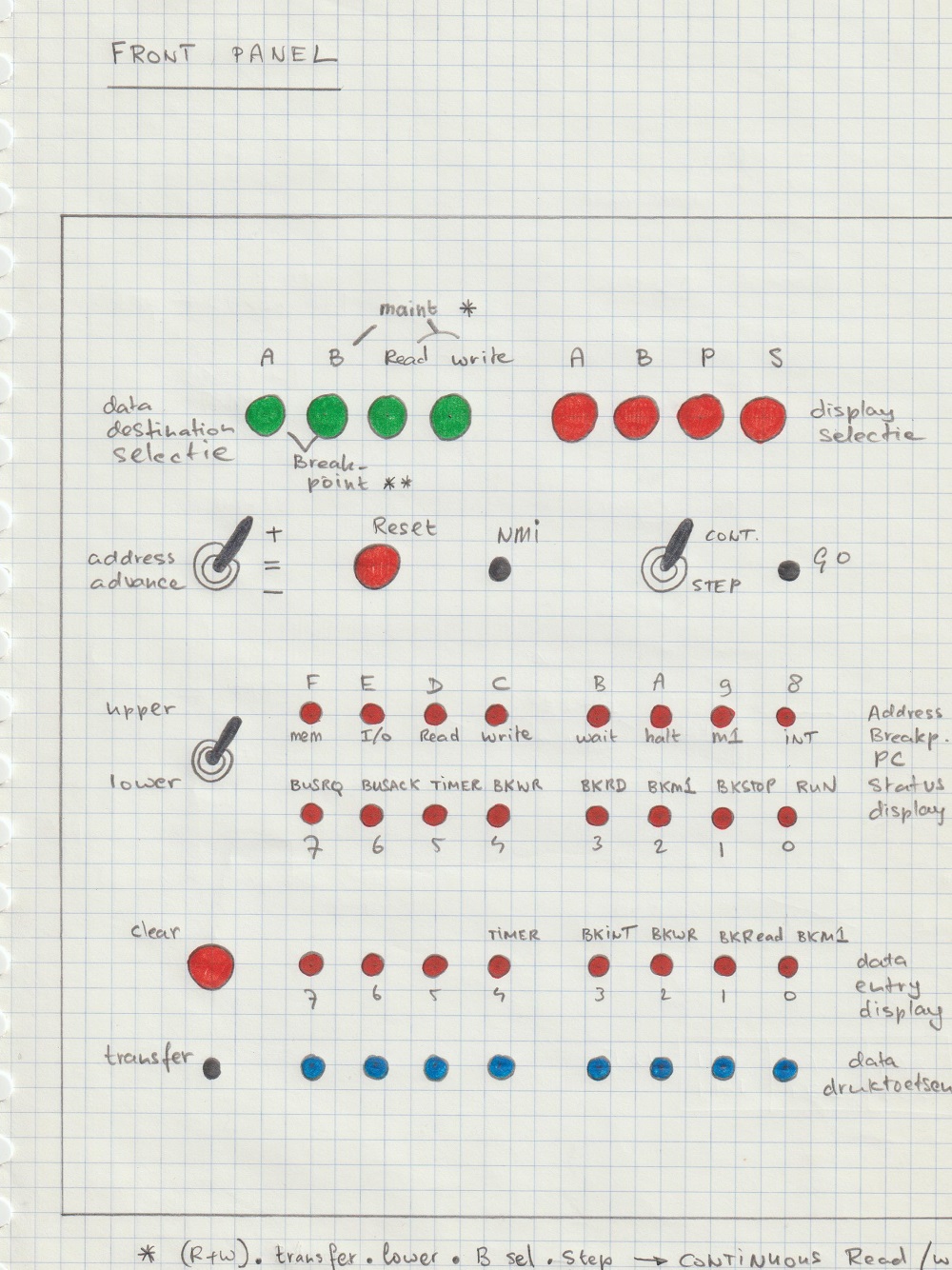
The Z80 has an 8 bit data- and 16 bit address bus.
The console shows 8 LEDs for data and 16 for addresses, breakpoints, status
and display of the processors P (instruction address) register.
Also there are switches for display selection, step-mode, GO, NMI (non masked interrupt).
Data is entered in the data register by push-buttons. (lower page).
This data may be transferred to the lower- and upper address register or to memory using this address.
The address is incremented/decrementd after a memory transfer.
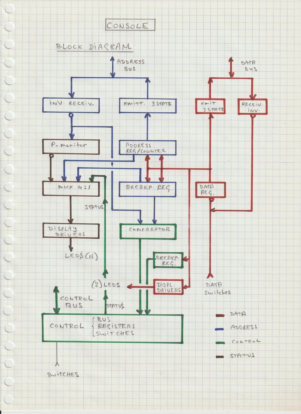
Here is the block diagram of the console:
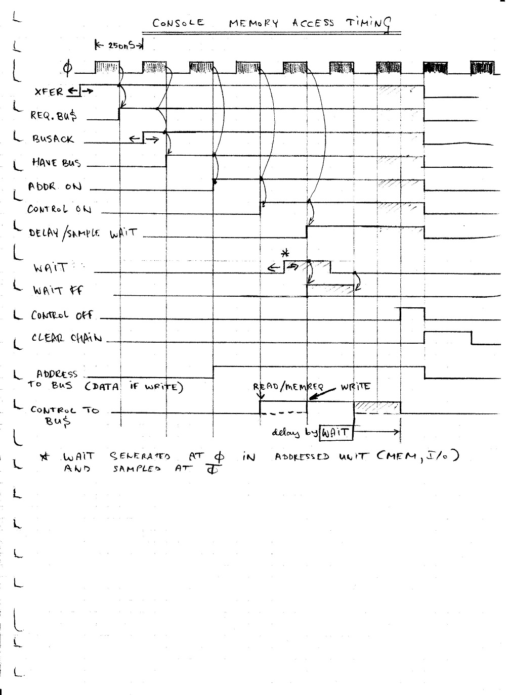
And the timing for data transfers:
Diagrams will follow later.
 To CPU diagrams